Tutorial 1: | TM Cutoff Frequencies of a Rectangular Waveguide |
Objective: Find the cutoff frequencies of the first three TM-modes in a WR(28) rectangular waveguide. Assume perfectly conducting walls. The guide is filled with air.
This standard rectangular waveguide has the following inner dimensions:
a = 0.28 in, b = 0.14 in.
1.1 Preliminary Considerations
At cutoff, all field components are independent of position along the longitudinal axis of the guide (y-axis). Thus, we need to solve a genuine 2D problem. MEFiSTo-2D is perfectly suitable for this task.
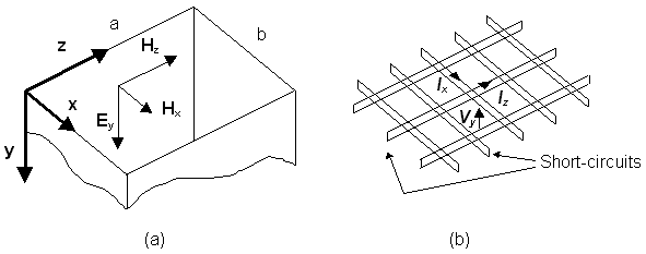
![]()
Figure 2-1 (a) Cross-section of the waveguide showing the co-ordinate axes and the field components of the TM-modes at cutoff. These components are independent of y. (b) Isometric view of a shunt-connected transmission line network (TLM mesh) used to model the field behavior in the cross-section. The sidewalls of the guide are modeled by short-circuits We model the longitudinal Ey-field of the TM modes by the voltage Vy in the TLM mesh. (Vy is perpendicular to the screen). The transverse magnetic field components are then modeled by the currents in the TLM mesh (see Figure 2-1). The correspondence is as follows:
- The mesh voltage Vy models the electric field component Ey.
- The mesh current Iz models the magnetic field component -Hx
- The mesh current Ix models the magnetic field component Hz
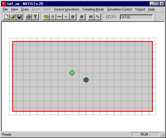
We discretize the cross-section of the waveguide into square cells. As a rule of thumb, the mesh size should be smaller than 1/10th of the shortest wavelength. 10 cells along the shortest dimension of the waveguide cross-section should be about right for a first evaluation. Obviously, the discretization in Figure 1 is much too coarse.
We thus discretize the waveguide into 20 x 10 cells of size 0.014 in x 0.014 in = 0.3556 mm x 0.3556 mm.
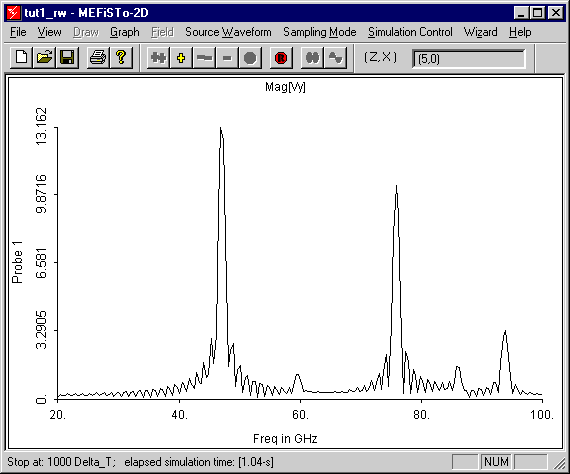
The cutoff frequencies of the TM-modes are interpreted as the eigenfrequencies (transverse resonance frequencies) of a field that is uniform in y-direction
1.2 Define and Input the Structure Set up the TLM mesh and draw the waveguide cross-section into the discretized TLM mesh. Proceed as follows:
1.2.1 Start MEFiSTo-2D
- Click Start on the task bar,
- Point to Programs > MEFiSTo-2D > MEFiSTo-2D. The program starts up. A screen with an array of 17 by 11 squares appears. This is the default TLM mesh.
1.2.2 Create a new mesh
- In the File menu, select New,
- In the Mesh New dialog box, set
Number of cells in Z-direction: 21 Number of cells in X-direction: 11 Cell size Delta L in [mm]: 0.3556 Note: Always choose a mesh that is at least one cell larger than the structure you want to implement. (The waveguide cross-section is 20x10 cells).
- Click OK.The new mesh appears.
1.2.3 Draw the guide walls
- In the Draw menu, select Electric Wall,
- Point to the center of the top-left square. (z,x) = (0,0),
- Hold down the left mouse button, drag the cursor horizontally to the top-right square (z,x) = (20,0) and release. The horizontal red line is the top wall of the waveguide.
- Point to the center of the top-right square (z,x) = (20,0),
- Hold down the left mouse button, drag the cursor vertically down to the center of the bottom-right square (z,x) = (20,10) and release. The vertical red line is the right sidewall.
- Draw the bottom wall and the left side wall using the same procedure. The drawing of the guide cross-section is complete.
Note: The mesh lines on the screen represent TLM transmission lines, seen from above. The points where the lines intersect are called Nodes. A square area containing a node in its center is a Cell. Regular boundaries are usually inserted halfway between nodes and thus coincide with cell boundaries (see also Fig. 2-1 in the "MEFiSTo-2D Theory" booklet).
- Check that you have indeed drawn an area containing 20 x 10 cells.
1.2.4 Define the Computation Region and its properties
The program does not automatically assume that you want to compute the field in all cells. You must therefore specify which cells should be "alive", and what should be the electromagnetic properties of the space they occupy.
- In the Draw menu, select Computation Region.
- Point to the center of the top-left square: (z,x) = (1,1)
- Hold down the left mouse button, drag the cursor diagonally to the center of the bottom-right square: (z,x) = (20,10) and release. The area covered turns gray, and a dialog box appears.
- In the dialog box, set
Relative dielectric constant: 1 Conductivity [S/M]: 0 Note: Every cell of the computational domain must be contained in a computation region. The background permeability and permittivity are assumed to be those of free space, m0 and e0.
- Click OK. The drawing is complete
1.2.5 Create a source point and a probe
Just like in a measurement you must excite the fields inside the waveguide by injecting energy into it. You must also sample the field response to the excitation. The simplest way to do this is to create a Source Point for excitation and a Probe for sampling the field response. The positioning of the source point and the probe is governed by the same principles as the positioning of real input and output devices in a measurement.
1.2.5.1 Create a Source Point
Let us first place a single source point into the guide cross-section and inject the y-directed electric field component. The position of the source point will, of course, determine what modes will be excited, and how strongly. Placing the source in the center of the waveguide will excite only modes with an even symmetry about the center (TM11, TM31, TM51, TM13, TM33, etc,) and thus exclude the modes with odd symmetry. We will thus place the source point slightly off-center to excite as many modes as possible.
- In the View menu, select Draw,
- In the Draw menu, select Source Point,
- Place the cursor on node (9,5) and click the left mouse button once. A source point appears, and a dialog box comes up. Accept the default values (Scaling Factor = 0.707107, Node Voltage Vy) by clicking on OK.
Note: In the shunt-connected TLM network, the node voltage Vy emulates the Electric Field component Ey. By injecting one or several voltage impulses into the TLM mesh at this point we simulate the injection of an electric field using a y-directed antenna.
1.2.5.2 Create a Probe
- For the placement of a sampling probe, the same considerations apply regarding the positioning. We will thus choose a slightly off-set position for the probe.
- In the Draw menu, select Probe,
- Place the cursor on node (11,6) and click the left mouse button once. A source point appears.
- Save your structure using the Save or Save As command in the File menu. (The extension tlm is automatically added to the filename.)
The screen should now look like Figure 2-2.
Figure 2-2: View of the TLM mesh in the cross-section of the waveguide.
1.3 Perform the Simulation
You may have noticed that the
and
buttons in the Simulation Bar have turned yellow, indicating that simulation is now enabled and that all elements necessary for a simulation have been created. A few more decisions need to be made, though.
1.3.1 Select a Source Waveform
Having chosen a standard waveguide problem as our first exercise, we know already the solution with perfect accuracy. But let us assume for the moment that we do not know it yet. We therefore inject a signal with an extremely wide bandwidth to be certain that all relevant frequencies are excited. This signal will be a single voltage impulse.
- In the Source Waveform menu, select Impulse (T).
- In the dialog box, accept the default value (Magnitude = 1). A graph showing the source waveform appears on the screen. It is a single impulse of amplitude 1 at t = 0. The time scale is in multiples of the time step Dt. (We will learn later how to change these scales).
1.3.2 Select a Sampling Mode
The Sampling Mode menu allows you to select the quantity you want to sample with your field probe. This time we choose to sample the same component that we have injected, namely the node voltage Vy (equivalent to the longitudinal field component Ey in the waveguide cross-section).
- In the Sampling Mode menu, select Vy == Ey.
1.3.3 Set Simulation Control Data
The Simulation Control menu allows you to specify the simulation process in detail.
- In the Simulation Control menu, select Control Data. The Simulation Control Data dialog box appears.
- In the Time Domain Data group box, enter the total duration of the simulation (1000 time steps) and the update interval (50 time steps).
Note: Since we will perform a transient solution in the time domain, we must choose a sufficient number of time steps to reach a quasi-steady state. As a very rough rule of thumb, multiply the largest dimension in Dl of the structure by 50 (20 x 50 = 1000). You can increase the number of time steps later, or stop the simulation earlier if you wish
- In the Frequency Domain Data group box, enter the number of frequency points (200), the lower frequency (20 GHz), and the upper frequency (100 GHz).
Note: Knowing that the lowest cutoff frequency of the WR(28) waveguide is about 21 GHz, our solutions will certainly lie above 20 GHz. The upper frequency value of 100 GHz is probably somewhat high, but we can narrow down the Fourier transform window later if necessary. Since the frequency range is rather large, 200 points will be a reasonable resolution. Again, we can change it later.
- In the TLM Mesh Data group box, verify the value of the mesh parameter Dl. The time step is automatically computed and cannot be changed since it is "hard-wired" and corresponds to the Courant stability limit in FDTD.
- In the TLM Dispersion Error in Percent group box, note that the error in the attenuation constant is zero since the dielectric in the waveguide is lossless. The maximum error in the phase constant is the upper bound of the dispersion error, calculated for the value of the Upper Frequency entered above. It is 1.23% in this case. We will see later that the actual error of our solutions is much lower than this worst-case value.
- Confirm the dialog box content by clicking OK.
We are now ready to start the simulation and to observe the process.
1.3.4 Start Simulation
- In the View menu, select Graph.
- In the Graph menu, select Probe Responses. You see three graphs for displaying the responses of Probe 1. The upper graph will be the time response, the middle graph will be the magnitude of the frequency response (discrete Fourier Transform), and the lower graph the phase response. Note that the horizontal scales correspond to the values set previously in the Simulation Control Data window.
- Start the simulation by clicking on the
button in the Simulation Bar. You see that the time response (upper graph) is displayed in bursts of 50 time steps, and that the magnitude and phase of the Fourier Transform are updated at the same rate. The whole simulation is completed within a few seconds.
Note: We can already distinguish five resonances in the range from 40 to 100 GHz. We will now inspect the frequency response more closely. If you would like to see the same simulation again, click the Reset Simulator button above the window, and then " ++ ".
- In the Graph menu, select Probe 1 > V(f) Magnitude. A single window displays the magnitude of the frequency response in greater detail. (See Figure 2-3)
![]()
Figure 2-3: Fourier Transform of the impulse response of the TLM mesh that models the cross-section of a WR(28) waveguide.
- With the mouse, point at each resonance peak and click the left mouse button. The first number in the Coordinate Area is the frequency in GHz, the second is the magnitude of the peak. The first three cutoff frequencies are approximately 47 GHz, 59.5 GHz and 75.9 GHz. These peaks are close to the analytically calculated cutoff frequencies of the following modes:
TM11 (fc1 = 47.128544 GHz) TM21 (fc2 = 59.613417 GHz) TM31 (fc3 = 75.992494 GHz) 1.4 Process and Improve the Simulation Results
While the results obtained so far are sufficiently accurate for the identification of the first cutoff frequencies, MEFiSTo-2D can achieve much better precision and resolution. The main limitation has been the low frequency resolution of the frequency axis. The next step will be to zoom in on the three first resonances to get a better reading of the position of the maxima.
1.4.1 Zoom in on the individual resonance peaks
- In the Graph menu, select Probe 1 > V(f) Magnitude.
- Place the cursor slightly to the left and above the first resonance peak. Press the left mouse button and draw a narrow rectangle that includes the peak. Then release the mouse button again. The rectangular area now fills the entire screen, and you see the peak in much greater detaill.
Note: If you are not happy with the area you have selected, you can return to the full view by returning to the Graph menu and selecting Probe 1 > V(f) Magnitude again. Now draw another rectangle. The frequency axis is now spread out, but the peak is still not well defined. In fact, you see a piecewise linear approximation of the resonance curve that is not sufficiently resolved to identify the exact position of the maximum. The solution is to increase the number of frequency points in the window as follows.
1.4.2 Recompute the Fourier Transform
- In the Simulation Control menu, select Recompute DFT,
- In the Frequency Domain Data group box, change the lower and upper frequency values to 45 GHz and 48 GHz, respectively, then click on OK.
- MEFiSTo-2D performs a new Discrete Fourier Transform of the impulse response. Note that it is not necessary to perform the TLM simulation again since the response is still in the computer memory.
- The resolution is now much higher since the 200 frequency points are now concentrated in a much narrower Fourier Transform window (3 GHz instead of 80 GHz).
- Determine the position of the maximum by clicking on it and reading the first number in the Coordinate Window. (~ 47.086 GHz). The theoretically exact value is 47.128544 GHz, thus the error is - 0.09%. This is three times more accurate than the maximum phase constant error value in the Simulation Control Data window.
- You can repeat the process again and narrow down the Fourier Transform window further. This will improve your resolution, but not necessarily the accuracy of your results. To verify this, you should increase the number of time steps of the TLM simulation and determine if this results in a shift of the resonance peak.
1.4.3 Increase the number of time steps
- In the Simulation Control menu, select Control Data,
- In the Time Domain Data group box, increase the total number of time steps from 1000 to 4000. Then click on OK.
- Click on the
button in the Simulation Bar.
- Observe the narrowing resonance curve.
- Determine the position of the maximum again by clicking on it and reading the first number in the Coordinate Window. (~ 47.086 GHz). There was no significant shift in the position of the maximum. This indicates that 1000 time steps were sufficient to reach the accuracy limit of the discrete waveguide model.
1.5 Add Another Probe
The second resonance peak at 60 GHz is not very pronounced as compared with the first and third. This is due to the position of the Probe with respect to the maximum of the mode field. Because the second peak is so small, the risk of error is greatly increased since the sidelobes (due to the Gibbs effect) of the first resonance may interfere with it and give rise to a substantial truncation error. The remedy is to place another Probe at a position where the field of the TM21 mode is larger.
- Reset the Simulator by clicking the Reset Simulator button at the top of the screen. This will allow you to edit the structure and to add new elements.
- In the View menu, select Draw,
- In the Draw menu, select Probe,
- Place the cursor on node (16,6) and click the left mouse button once. A second probe appears.
- Save your new structure using the Save as command in the File menu if you do not want to change the original file tut1_rw.tlm.
- Perform the simulation again by following the steps beginning at Section 1.3.3. You will now see two sets of time-and frequency responses. The frequency response of Probe 2 shows a much stronger response at 60 GHz than Probe 1.
- Determine the frequencies of the first three resonant peaks by recomputing the Fourier Transform for three narrow windows centered at the three peaks.
You should obtain approximately the following values:
fc1 ~ 47.096 GHz fc2 ~ 59.617 GHz fc3 ~ 75.922 GHz
1.6 Validation of Computed Results
Comparison of analytical values for the cutoff frequencies of the WR(28) waveguide with the simulation data yields the results shown in Table 2-1.
The errors turn out to be much smaller than the upper bound of the phase velocity error displayed in the Simulation Control Data box. If you want to reduce the dispersion error further, the only solution is to increase the number of cells in the cross-section of the waveguide. In fact, it is always a good idea to solve the same structure once or twice with an increasingly finer mesh. This allows you to verify if and how the solution converges to the ideal value for infinitesimal mesh size.
Note that when you double the number of cells in each coordinate direction, the number of cells and hence, the memory requirements increase by a factor 22 = 4. At the same time, the required number of time steps doubles, and the total computational expenditure thus grows by a factor 23 = 8.
Mode
Analytical Cutoff fc/GHz
MEFiSTo-2D fc/GHz
Relative Error in Percent
TM11 47.128544 47.096 -0.069 TM21
59.613417
59.617
0.006
TM31
75.992494
75.992
-0.0006
Table 2-1: Comparison of simulation results with analytically exact values.