Tutorial 2: | Propagation in Uniform Transmission Lines and Waveguides |
2.1 Preliminary Considerations
In this tutorial we will explore the propagation of electromagnetic fields in two types of uniform transmission lines, namely parallel-plate waveguides and rectangular waveguides. Since MEFiSTo-2D can only handle two-dimensional problems, the simulations are restricted to modes of propagation that depend on two space dimensions only, namely the TEM-mode in the parallel-plate waveguide, and TEm0-modes in both types of waveguides.
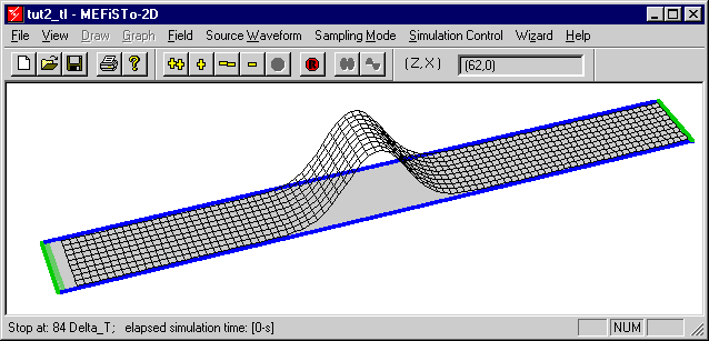
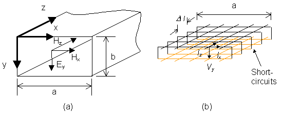
In contrast to the first tutorial where we studied the cutoff behavior of a rectangular waveguide as a transverse resonance phenomenon, we will now place the longitudinal axis of the waveguide along the z-axis. The node voltage Vy in the 2D shunt TLM network represents the transverse Ey component in the guide, while the currents in the mesh simulate the two companion magnetic field components. (Iz models -Hx, and Ix models Hz). This is shown in Figure 2-4.
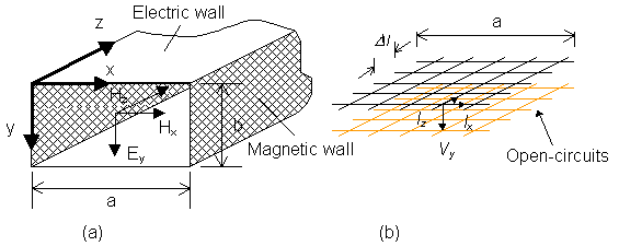
![]()
Figure 2-4: (a) View of the parallel-plate waveguide with magnetic sidewalls and orientation of the three field components of TEm0-modes propagating in z-direction. For m=0 we have a TEM mode with Hz = Ix = 0. (b) orientation of the TLM mesh and of the voltage and currents that model these modes. All field and network quantities are independent of y. The magnetic sidewalls are modeled by open-circuits. Top and bottom walls of the waveguides are thus parallel to the zx-plane, and their spacing b is of no consequence since we consider only those field quantities that are independent of y. Therefore, we draw only the footprint of the side walls that determine the topology of the guiding structure.
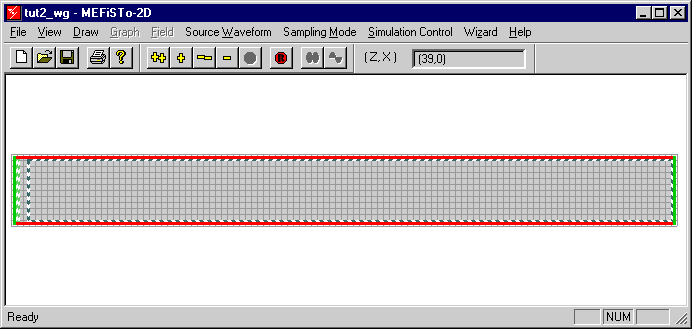
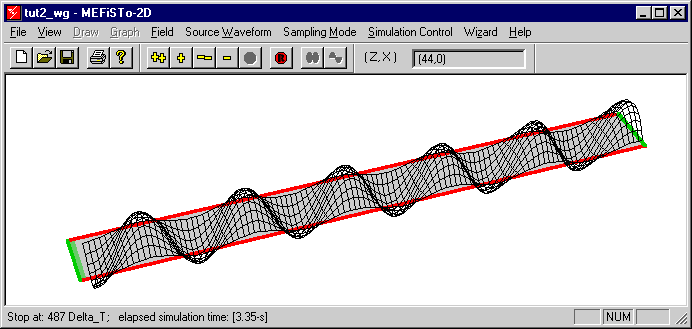
We will begin by studying the propagation of TEM fields in a parallel-plate waveguide.
2.2 TEM Propagation in Parallel-Plate Waveguide
Objective: Draw a parallel-plate waveguide, 10 mm wide and 90 mm long. Terminate it at both ends with a matched load. Study the propagation of TEM waves in this structure.
2.2.1 Create a new mesh
- In the File menu, select New,
- In the Mesh New dialog box, set
Number of cells in Z-direction: 91 Number of cells in X-direction: 11 Cell size Delta L in [mm]: 1 - Click OK.The new mesh appears.
2.2.2 Draw the magnetic side walls
- In the Draw menu, select Magnetic Wall,
- Draw the two magnetic side walls, one from point (0,0) to point (90,0), and the other from point (0,10) to point (90,10).
2.2.3 Define the computational domain and its properties
- In the Draw menu, select Computation Region,
- Fill the entire area of the guide with a single rectangle. In the dialog box, set Relative dielectric constant = 1, Conductivity [S/M] = 0. Click OK.
Note: The Computation Region not only defines the permittivity and conductivity of the medium, but also brings the TLM cells inside the box "alive". No computation is performed inside cells that are not covered by a Computation Region.
2.2.4 Draw the matched loads at both ends
- In the Draw menu, select Reflection Wall.
- Draw a Reflection Wall across both ends of the guide. In the dialog box, accept the default value TEM wave reflection coefficient = 0, which characterizes an absorbing boundary or matched termination for a TEM plane wave incident normally on the boundary.
Note: The Relative dielectric constant is by default the value specified when creating the last Computation Region. It is thus recommended to draw the Computation Region adjacent to an absorbing wall before drawing the wall itself. However, the dielectric constant can be changed at any time. Note that the Local impulse reflection coefficient (G i = -0.171573) is different from 0 as predicted by 2D-TLM Theory.
2.2.5 Draw a source region
- In the Draw menu, select Source Region,
- Draw a narrow vertical box around the left-most column of nodes inside the guide. In the dialog box, accept the default Scaling Factor of 0.707107, which is the value required to launch a voltage wave of 1 V in the input ports. The source distribution is constant in x-direction.
Note: Creating a source region with a constant spatial field distribution in x-direction is equivalent to entering a column of single source points, each having the same weight. This type of source region is suitable for launching a uniform plane wavefront.
2.2.6 Draw an animation region
To observe and visualize the fields in the waveguide, we sample the node voltages and currents in a rectangular region and display their distribution dynamically. We will first determine the display area by drawing an animation region. We then inject a source waveform at the source region and view the fields.
- In the View menu, select Draw,
- In the Draw menu, select Animation Region,
- Draw a box from point (3,1) to point (90,10).
You should now see the picture shown in Figure 2-5
![]()
Figure 2-5: Discretized parallel-plate waveguide with magnetic sidewalls and matched loads at each end. The source is a narrow source region at the left extremity. An animation region covers the bulk of the guide
2.2.7 Simulate and visualize TEM wave propagation
- In the Source Waveform menu, select Gaussian (T) In the dialog box, set Magnitude = 1, Sigma in Delta_t = 6, and Mean in Delta_t =24. Click OK. The waveform appears on the screen.
- In the Sampling Mode menu, select Vy == Ey.
- In the Simulation Control menu, select Control Data. In the dialog box, set Total number of time steps = 180, and Time steps between updates = 1. Disregard the Frequency Domain Data group box. and click OK.
- In the View menu, select Field. A three-dimensional view of the guide in its TLM mesh appears on the screen.
- In the Field menu, select Field Display Attributes. Shift, rotate and scale the display until you like it.
- Start the simulation by clicking on the
button.
- Observe the field as it propagates through the structure. Continue to modify the 3D View Parameters while the program is running. Adjust the magnification of the field using Magnify Y or Reduce Y. Change the size of the MEFiSTO-2D client window. Stop and start the simulation again, or step forward one step at a time using the
button.
![]()
Figure 2-6: Field display of a Gaussian Pulse traveling through a parallel-plate waveguide with magnetic side walls. A TEM wave is created by implementing a source region with a uniform transverse distribution.
- You can also change the update interval in the Simulation Control Data box while the simulation is stopped or running. This will change the speed of the field animation at the expense of smoothness. Try also the hidden line removal feature by deselecting the Wire Frame box.
- To visualize the magnetic field components in z- and x-direction, change your selection in the Sampling Mode window while the simulation is running or stopped.
2.3 TE
10 Propagation in Rectangular Waveguide
Objective: Draw a WR(90) rectangular waveguide, 0.9 in wide and 9 in long. Terminate it at both ends with a matched load. Study the propagation of TE10-waves in this structure.
2.3.1 Create a new mesh
The Ey-component of the TE10-mode has a half-sinusoidal distribution in the cross-section of the waveguide. Discretizing the cross-section into 11 cells will be more than adequate (we should have at least 10 cells per wavelength, or 5 cells per half-wavelength.)
Figure 2-7 : | (a) | View of the rectangular waveguide with electric side and broad walls and orientation of the three field components of TEm0-modes propagating in z-direction. |
(b) | Orientation of the TLM mesh and of the voltage and currents that model these modes. All field and network quantities are independent of y. The electric sidewalls are modeled by short-circuits. Note that the mesh in the figure is only 5 Dl wide for better clarity. |
The waveguide will thus be discretized into 11 x 110 cells, with a
Dl of 0.9 x 25.4/11 mm = 2.078182 mm
- In the File menu, select New,
- In the Mesh New dialog box, set
Number of cells in Z-direction: 111 Number of cells in X-direction: 12 Cell size Delta L in [mm]: 2.078182
- Click OK. The new mesh appears.
2.3.2 Draw the electric side walls
- In the Draw menu, select Electric Wall,
- Draw two electric side walls, one from point (0,0) to point (110,0), and the other from point (0,11) to point (110,11).
2.3.3 Define the computational domain and its properies
- In the Draw menu, select Computation Region,
- Fill the guide with a single rectangle. In the dialog box, set Relative dielectric constant = 1, Conductivity [S/M] = 0. Click OK.
2.3.4 Draw the matched loads at both ends
Here we face a serious problem. Since the TE10-mode wave impedance is frequency-dependent, a wall with a fixed impedance can represent a matched load only at one single frequency. (We will see later how we can solve this dilemma using the Johns Matrix wall). For now, let us select a frequency f = 10 GHz and determine the matching impedance at that frequency using the formula
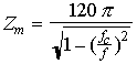
where fc = 6.55714 GHz.
Thus, at 10 GHz we have Zm = 499.32 Ohms.
For your convenience, these formulae have been implemented in a handy calculator called "Waveguide Wizard". To use this tool, open the Wizard menu, select "Waveguide" and enter the waveguide data. You can cut and paste the results from the Wizard into the data field of the Reflection Wall dialog box using the Ctrl+C and Ctrl+V commands.
- In the Draw menu, select Reflection Wall,
- Draw a Reflection Wall across both ends of the guide, from (0,0) to (0,11) and from (110,0) to (110,11). In the dialog box, press the radio button in front of Wall impedance in Ohms and enter (or paste) 499.32 which represents a narrowband absorbing boundary, or matched load, for a TE10-mode at 10 GHz.
2.3.5 Draw a TE10 source region
- In the Draw menu, select Source Region,
- Draw a narrow vertical box around the left-most column of nodes inside the guide. In the dialog box, accept the default Scaling Factor of 1. In the Spatial Distribution field, select Half Sin to launch the TE10-mode.
Note: Creating a source region with a half sine spatial field distribution in x-direction is equivalent to entering a column of single source points, each having a magnitude of excitation weighted by a half-sine function in x-direction. This type of source region is suitable for launching a pure TE10-mode wavefront.
2.3.6 Draw an animation region
- In the View menu, select Draw,
- In the Draw menu, select Animation Region,
- Draw a box from point (3,1) to point (110,11).
The screen should look like as in Figure 2-8.
![]()
Figure 2-8: Discretized rectangular waveguide with electric sidewalls and narrowband matched loads at each end. The source is a narrow source region at the left extremity. An animation region covers most of the guide.
2.3.7 Simulate and visualize TE10 wave propagation
- In the Source Waveform menu, select Sin (f). In the dialog box, set Magnitude = 1, Frequency [GHz] = 10. Click OK. The waveform appears on the screen.
- In the Sampling Mode menu, select Vy == Ey
- In the Simulation Control menu, select Control Data. In the dialog box, set Total number of time steps = 1000, and Time steps between updates = 1. Disregard the Frequency Domain Data group box and check that the cell size is correctly entered. Then click OK.
- In the View menu, select Field. A three-dimensional view of the guide in its TLM mesh appears on the screen.
- In the Field menu, select Field Display Attributes. Shift, rotate and scale the display until you like it.
- Start the simulation by clicking on the
button.
- Observe the field as it propagates through the structure. Continue to modify the 3D View Parameters while the program is running. Adjust the magnification of the field using Magnify Y or Reduce Y. Change the size of the MEFiSTO-2D client window. Stop and start the simulation again, or step forward one step at a time using the
button.
Figure 2-9: Electric field Ey in the waveguide at 10 GHz after 487 time steps.
- You can also change the update interval in the Simulation Control Data box while the simulation is stopped or running. This will change the speed of the field animation at the expense of smoothness. Try also the hidden line removal feature by deselecting the Wire Frame box.
- To visualize the magnetic field components in z- and x-direction, change your selection in the Sampling Mode window while the simulation is running or stopped.
Note: Since the sinusoidal excitation is a "hard" sine that starts abruptly at t = 0, the transient response of the guide is dispersive, resulting in a "precursor" and some initial ringing at the cutoff frequency. However, after several hundred time steps the propagating wave is stabilized and appears to be fully absorbed by the load at the far end.