| Tutorial
3: |
Analysis of a Microstrip
Lowpass Filter |
Tutorial Example File:
tut3_mlf.tlm
3.1. Preliminary
Considerations
The file tut3_mlf.tlm contains
data for a microstrip lowpass filter modeled by its
equivalent parallel-plate waveguide model with magnetic
sidewalls and non-dispersive effective permittivity. (This
model has, of course, certain limitations but works well at
low frequencies, in this case several GHz).
Several empirical formulae have been
developed over the years to calculate the properties of the
equivalent parallel-plate waveguide from the microstrip
charactristics. Figure 1 shows the cross-sections of a
microstrip line and its equivalent model that can be
implemented in 2D since all field quantities are independent
on the vertical direction.
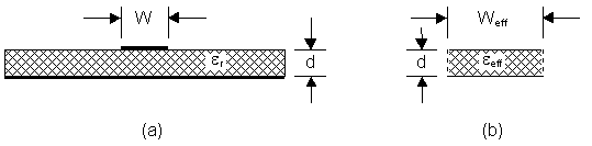
| Figure 2-10: |
(a) |
Cross-section
of a microstrip line. |
| (b) |
Its
equivalent parallel plate waveguide model with
magnetic sidewalls. |
For convenience, such formulae have
been implemented in the Microstrip Wizard that you can
find under the Wizard menu. Simply key in the
substrate thickness d, the relative dielectric
constant of the substrate, er , followed by either the strip
width W, the normalized strip width W/d, or the
microstrip characteristic impedance Z0m.
The Wizard then yields the effective width and
effective dielectric constant that you can implement in the
TLM model.
The topology of the filter appears on
the screen as soon as the file tut3_mlf.tlm is opened.
Magnetic walls (blue) define the geometry of the filter. The
filter is terminated at both ends by reflection walls
(green); the reflection coefficient of these walls has been
chosen such that the input and output ports of the filter are
matched. Note that the impedance of the absorbing walls is
not equal to the microstrip characteristic impedance but
rather the TEM wave impedance in the medium that fills the
parallel plate waveguide, namely h 0/Ö eeff . A reference section with the
same electrical properties as the input section is needed for
the extraction of the S-parameters of the filter. This
reference section appears below the filter input. Both the
filter and the reference section are filled with dielectric
or computation boxes, as indicated by the darker color.
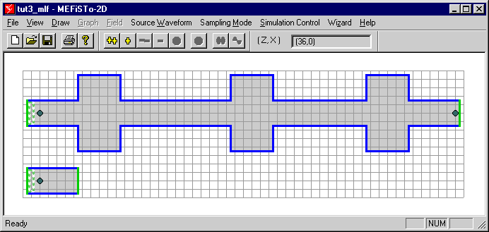
| Figure
2-11: |
Microstrip lowpass filter
implemented as a parallel-plate waveguide structure
with magnetic sidewalls, and reference structure for
the extraction of scattering parameters. |
3.2 Define and Input the
Structure
If you want to re-create the geometry
of the lowpass filter, follow this recommended input sequence
so that the program generates the proper values for the
reflection coefficients of the reflection walls.
3.2.1 Create a new mesh
- In the File menu, select New,
- In the Mesh New dialog box,
enter
Number of cells in Z-direction: 52
Number of cells in X-direction: 15
Cell size Delta L in [mm]: 1
- Click OK. The new mesh appears.
3.2.2 Draw the magnetic
walls
- In the Draw menu, select
Magnetic Wall,
- Draw the magnetic wall
sections using the counter in the Coordinate Area.
The coordinates of the wall sections can be extracted
from the Graph window of file tut3_mlf.tlm
3.2.3 Define the computational domain
- In the Draw menu, select Computation
Region,
- Fill all rectangular subareas of
the filter and the reference structure with
contiguous Computation Regions. In each dialog box,
set Relative dielectric constant = 8.22146,
Conductivity [S/M] = 0.
| Note: |
If
you do not want to redraw the structure, you can at
least check the property of each element of .the
filter. Proceed as follows: |
- In the Draw menu, choose Select
Element.
- Point and click on any
element or area of the filter. The selected element
turns purple, and the name of the element appears in
the Status Bar.
- In the Right-Mouse-Button
menu, select Property. A dialog box displays
the properties of the element, if these properties
have previously been specified through a dialog box.
3.2.4 Draw the reflection
walls
- In the Draw menu, select Reflection
Wall,
- Draw a Reflection Wall at
both ports of the filter and the reference structure.
In each dialog box, accept the default value TEM
wave reflection coefficient = 0, which
characterizes an absorbing boundary or matched
termination for a TEM plane wave incident
normally on the boundary.
| Note: |
The Relative
dielectric constant is by default the value
specified when creating the last Computation
Region. It is thus recommended to draw the Computation
Region adjacent to an absorbing wall before
drawing the wall itself. However, the dielectric
constant can be changed at any time. Note that the
local impulse reflection coefficient (G i =-0.604351) is different
from 0 as predicted by 2D-TLM Theory. |
3.2.5 Draw the source
regions
- In the Draw menu, select Source
Region,
- Draw a narrow vertical box around
the left-most column of nodes inside the filter and
the reference structure. In the dialog box, accept
the default value of 2.02749 which is the
scaling factor required to launch a voltage wave of 1
V in the input ports. The source distribution is
constant in x-direction.
3.2.6. Place the probes
Up to three probes can be implemented
in MEFiSTo-2D. The probes are numbered by the
computer in the order in which they are have been created (1
to 3). If one of them is removed, the order is changed in
a complicated manner due to internal stack manipulation. In
this example, Probe 1 is the probe in the reference
section. Probe 2 and Probe 3 are placed in the
input and output ports of the filter. (Verify the numbering
of the probes by clicking on them after activating Select
Element in the Draw menu. The Status Bar
indicates the number of the probe.
Note: The
reference planes for the S-Parameters are defined by the
position of the probes.
3.3. Perform the Simulation
3.3.1. Select a Source
Waveform
As in the first tutorial example we
inject a signal of maximum bandwidth to be certain that all
relevant frequencies are excited. This signal will be a
single voltage impulse.
- In the Source Waveform
menu, select Impulse (T).
- In the dialog box, accept the
default value (Magnitude = 1). A graph showing
the source waveform appears on the screen.
3.3.2. Select a Sampling
Mode
Again, we choose to sample the same
component that we have injected, namely the node voltage Vy
(equivalent to the field component Ey
in the structure.
- In the Sampling Mode menu,
select Vy == Ey.
3.3.3. Set Simulation
Control Data
- In the Simulation Control
menu, select Control Data. The Simulation
Control Data dialog box appears.
- In the Time Domain Data
group box, select the total duration of the
simulation (2048 time steps) and the update interval
(50 time steps).
- In the Frequency Domain Data
group box, enter the number of frequency points (101),
the lower frequency (0 GHz), and the upper
frequency (6 GHz).
| Note: |
Since the structure
under test is a lowpass filter, we include the low
frequency range down to DC. The source waveform
(impulse) has a DC component as well. |
- In the TLM Mesh Data group
box, verify the value of the mesh parameter Dl. The time step is automatically
computed and cannot be changed. It guaranties
unconditional stability of the algorithm.
- In the TLM Dispersion Error in
Percent group box, note that the error in the
attenuation content is zero since the dielectric in
the waveguide is lossless. The maximum error in the
phase constant is the upper bound of the dispersion
error, calculated for the value of the Upper
Frequency entered above. It is 0.52% in
this case.
- Confirm the dialog box content by
clicking OK.
You are now ready to start the
simulation and to observe its progress. The screen should
look as in Figure 2-12.
3.3.4 Start Simulation
- In the View menu, select Graph.
- In the Graph menu, select Probe
Responses. You see three columns of graphs for
displaying the responses of Probes 1, 2, and 3.
The upper row of graphs will be the time response,
the middle row will be the magnitude of the frequency
response (discrete Fourier Transform), and the lower
row the phase response. Note that the horizontal
scales correspond to the values set previously in the
Simulation Control Data window.
- Start the simulation by clicking
on the
 button in the Simulation Bar. The time response
(upper row of graphs) is displayed in bursts of 50
time steps, and the magnitude and phase of the
Fourier Transform are updated at the same rate. The
whole simulation is completed within a few seconds.
button in the Simulation Bar. The time response
(upper row of graphs) is displayed in bursts of 50
time steps, and the magnitude and phase of the
Fourier Transform are updated at the same rate. The
whole simulation is completed within a few seconds.
| Note: |
The frequency
response of Probe 3 shows already the characteristics
of a lowpass filter from 0 to 1.5 GHz, with a
second passband centered around 4 GHz. The spectrum
of the voltage in the reference section is almost
flat. |
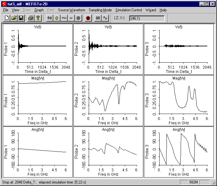
| Figure
2-12: |
Display of the probe
responses after 2048 time steps. . Top row:
Time responses of probes 1 to 3. Middle row:
Frequency responses (Discrete Fourier Transform) of
the probes 1 to 3. Bottom row: Phase responses
of the same. |
- In the Graph menu, select Probe
1 , 2, or 3 to inspect each of the nine windows
in greater detail.
| Note: |
The frequency domain
responses are not smooth but show a pronounced ripple
(Gibbs effect), particularly towards the higher
frequencies. This is due to the following reasons:
| a) |
The number of
time steps chosen (2048) is
insufficient. |
| b) |
The spectrum
of the source waveform contains frequencies
above the range of interest (0 - 6 GHz). |
|
1.4. Extract Scattering
Parameters
Before extracting scattering parameters
we must verify that the three probes are assigned to the
correct ports of the structure.
- In the Graph menu, select Port
Attributes.
- Verify in the dialog box that
| Probe 1 is
assigned to the Reference Port, |
| Probe 2 is
assigned to the Input Port, and |
| Probe 3 is
assigned to the Output Port of the filter.. |
- Verify also that TEM
mode propagation is selected for all ports, and that
they all have the same width. (If all ports have the
same width and carry the same mode, the value entered
for the width is immaterial, provided it is the same
for all ports.)
- In the Graph
menu, select S11 > Magnitude. The magnitude
of S11 is displayed. Note
again the ripple.
- In the Graph
menu, select S11 > Phase. The phase of S11
is displayed.
- In the Graph
menu, select S21 > Magnitude. The magnitude
of S21 is displayed. Note
again the ripple.
- In the Graph
menu, select S21 > Phase. The phase of S21
is displayed.
- To change the title,
axes or scales of these graphs, select Graph
Display Attributes under the Graph menu.
You may also display the S-parameters in dB
and as a Bar Graph by checking the appropriate boxes.
1.5. Simulation with a
reduced bandwidth source
To smoothen the S-parameter
curves, we will repeat the simulation with a source waveform
tailored to the frequency range of interest. Proceed as
follows:
- Reset the simulator by clicking
the Reset button.
- In the Source Waveform
menu, select Gaussian (f),
- In the dialog box, enter Magnitude
= 1, Bandwidth = 12, and Gaussian-Modulated
Carrier = Constant. Click OK, and inspect
the resulting Gaussian waveform. It is a signal with
a bandwidth ranging from -6 GHz to + 6 GHz, centered
about DC.
| Note: |
Even though the
properties of the signal have been defined in the
frequency domain, the time domain waveform will be
displayed. You can verify the spectral
characteristics of the signal by computing its
Fourier Transform. Simply create a short section of
TEM transmission line, match it at both ends, and
enter a source point and a probe. Then perform a TLM
simulation for a sufficient number of time steps and
look at the frequency response of the probe. In this
way you can use MEFiSTo-2D as a
spectrum analyzer for any discretized signal |
- In the Graph menu, select S21
> Magnitude,
- Start the simulation by clicking
the
button.
- Observe the convergence of the S21
graph. The curve is smoother at lower frequencies,
but the ripple at higher frequencies still persists.
We must increase the number of time steps further.
- In the Simulation Control
menu, select Control Data,
- In the Time Domain Data
field, set the Total number of time steps to 3000
and click OK.
- Start the simulation. The curve
becomes smooth.
You can now refine the resolution of
all graphs and study all aspects of the filter response in
greater detail by repeating the steps discussed in Tutorial
1. However, we will explore one more feature of MEFiSTo-2D,
namely its capability to dynamically display and visualize
the fields in the filter.
1.6. Visualize the
Electromagnetic Fields in the Filter.
If we want to observe the behavior of
the filter at a certain frequency, we can excite the filter
with a sinusoidal waveform at that frequency and visualize
the field as it propagates through the structure. Suppose we
are interested in the filter behavior at 1.6 GHz, which is
the upper edge of the first passband.
- Reset the simulator,
- In the View menu,
select Draw,
- In the Draw menu,
select Animation Region,
- Draw a box from point (2,1) to
point (51,9).
- In the Source Waveform
menu, select Sin (f). In the dialog box,
set Magnitude = 1 and Frequency [GHz] =
1.6. Click OK. The waveform appears on
the screen.
- In the Sampling Mode
menu, select Vy == Ey.
- In the Simulation Control
menu, select Control Data. In the dialog
box, set Total number of time steps = 1000,
and Time steps between updates = 1.
Disregard the Frequency Domain Data group
box and click OK.
- In the View menu,
select Field. A three-dimensional view of
the filter in its TLM mesh appears on the screen.
- In the Field menu,
select Field Display Attributes. Keep that
command box open on the side of the screen.
- Start the simulation by
clicking on the button.
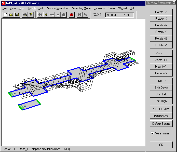
| Figure
2-13: |
Visualization of the electric
field Ey in the lowpass
filter at 1.6 GHz. Note that the field is
almost uniform over the wide sections of the
structure, indicating that they act essentially as
lumped capacitances at that frequency. The Wire Frame
option has been de-selected. |
- Observe the field as it propagates
through the structure. Shift, rotate and scale the
display until you like it. . Change the size of the MEFiSTO-2D
client window. Continue to modify the 3D View
Parameters while the program is running. Adjust the
magnification of the field using Magnify Y or Reduce
Y. Stop and start the simulation again, or step
forward one step at a time using the "+"
button.
- You can also change the update
interval in the Simulation Control Data box
while the simulation is stopped or running. This will
change the speed of the field animation at the
expense of smoothness. Try also the hidden line
removal feature by deselecting the Wire Frame
box.
- To visualize the magnetic field
components in z- and x-direction,
change your selection in the Sampling Mode
window.
You have now explored most, but not all
features of MEFiSTo-2D. These will be invoked
in the following tutorials.