This file contains data for an elementary varactor diode frequency multiplier. The structure consists of a parallel plate waveguide (two-dimensional microstrip model) with magnetic sidewalls (blue) and matching TEM boundaries (yellow) at each end. A Source Region for injecting a plane wave is visible on the left.
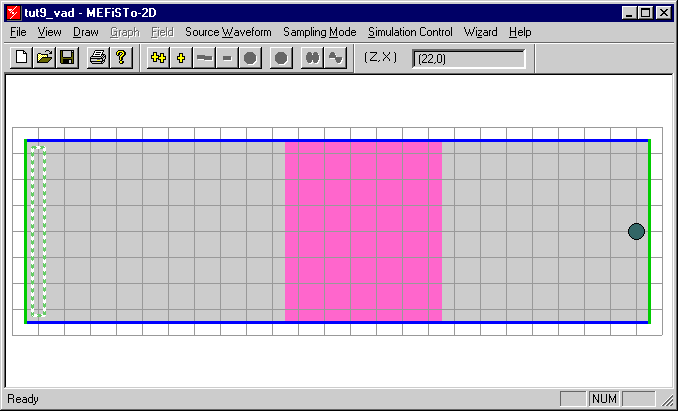
| Figure 2-25: | View of the parallel-plate waveguide section containing a rectangular Varactor Diode section. |
The diode model is the central among the three computation boxes. For simplicity it is rectangular rather than a circular. In a practical simulation it is recommended to draw a rectangular diode that has the same cross-sectional area as its circular counterpart. The 6 x 7 diode area has been created using the Varactor Diode item in the Draw menu. Its characteristics have been input at that time, and you may modify them at the beginning of a simulation, or review them after a simulation, by means of the Varactor Diode item in the View menu.
The other two computation regions are regular passive sections of parallel-plate waveguide. Remember that all data defining a structure can always be stored and displayed or printed by creating a rep ASCII file using the Save Text Report item in the File menu.
To start a simulation demonstrating the
generation of harmonic frequencies in a varactor diode, reset
the simulator and select a Sin(f) excitation at 10
GHz and a magnitude of 3V. In the Simulation
Control Data Box, verify that the mesh parameter Dl is 0.1 mm. Select the frequency range
from 0 to 40 GHz for the discrete Fourier transform, 301
frequency points, 4096 time steps, and an update
interval of 100 time steps between screen updates.
Then start the simulation by clicking on ![]() . Observe the distorted
waveform picked up at the probe 1 in the output port
(this is best observed by selecting Graph > Probe 1
>V(t), then display its spectrum (Graph > Probe
1 > V(f) Magnitude) which clearly exhibits higher
harmonic content at 20 and 30 GHz, as well as a
DC component (detected voltage) You can perform more
timesteps to minimize the Gibbs phenomenon and obtain narrow,
well-defined spectral lines, which may the be displayed or
printed.
. Observe the distorted
waveform picked up at the probe 1 in the output port
(this is best observed by selecting Graph > Probe 1
>V(t), then display its spectrum (Graph > Probe
1 > V(f) Magnitude) which clearly exhibits higher
harmonic content at 20 and 30 GHz, as well as a
DC component (detected voltage) You can perform more
timesteps to minimize the Gibbs phenomenon and obtain narrow,
well-defined spectral lines, which may the be displayed or
printed.
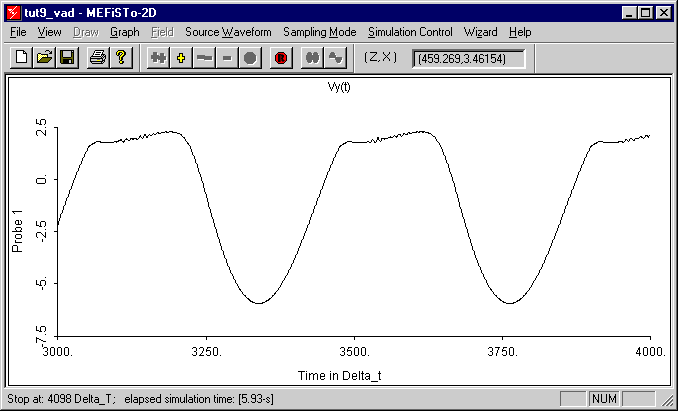
| Figure 2-26: | Output waveform of the waveguide section containing a Varactor Diode. The incident voltage is 3 V at 10 GHz. |
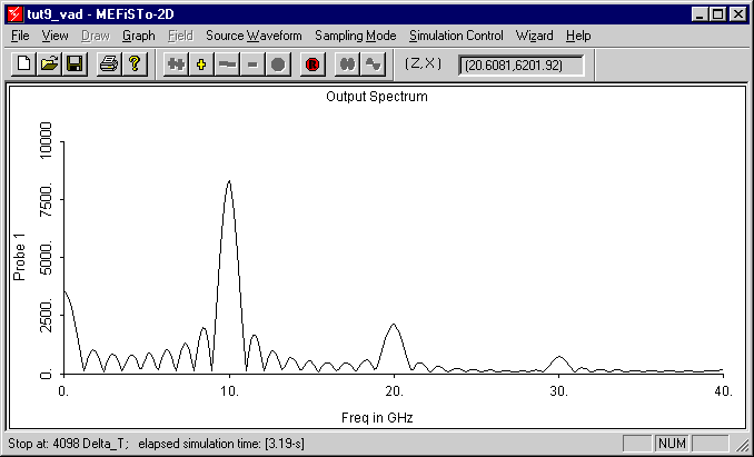
| Figure 2-27: | Spectrum of the waveform shown in Figure 2-26. Note the harmonics at 20 and 30 GHz as well as the DC component. |
The noise superimposed on the time domain output is due to spurious propagation effects within the nonlinear subregion. This effect can be controlled by increasing the time averaging period in the diode characteristics to 2 or more. To do this, reset the simulator, open the Varactor Diode item in the View menu and modify the value for the time averaging period. Then start a new simulation again.
A more complex example of parametric frequency halving using this nonlinear diode model is given in the Virtual Electromagnetics Laboratory.